There’s an old adage in manufacturing: “Cost, quality, and delivery: pick two.”
Like many old sayings, this is an oversimplification. Manufacturers can create a lower-cost, high-quality product with diminished lead time–even for complex products such as printed circuit boards (PCB). The key lies in careful planning and clever design, focusing on ease of manufacture.
The Manufacture of a PCB Consists of Four Cost Elements
- The PCB fabrication including copper, gold, epoxy and laminates.
- The electronic components on the bill of material.
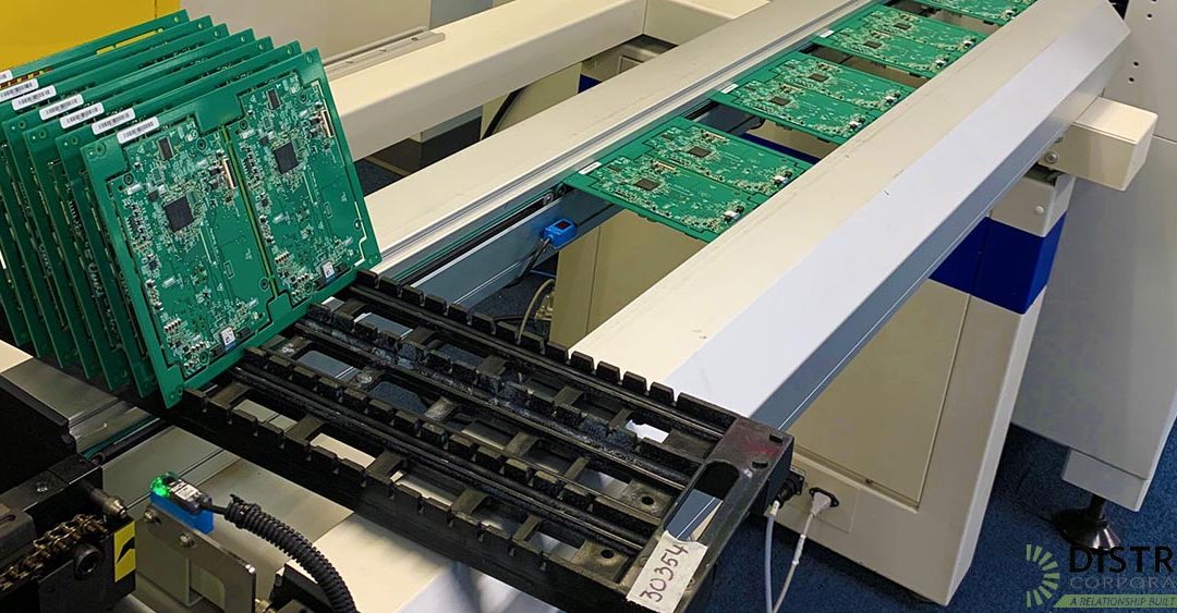
- The cost of assembling the components to the board.
- Testing the finished printed circuit board assembly.
Performing PCB Assembly? Follow Our Cost Saving Tips
Working with an experienced contract manufacturer allows companies to minimize the cost of fabrication, raw materials, assembly, and testing. Input from a good electronic contract manufacturer (ECM) will result in a lower cost PCB assembly that doesn’t sacrifice quality or functionality
When it comes to PCB assembly, cost and quality don’t have to be at odds. Have a question about the process? Our expertise provides the answer.
Reducing PCB Assembly Cost through Smart Design
The PCB is the centerpiece of a design. To minimize cost during fabrication, it is imperative to focus on a few key design principles. Including the following:
Aim for the smallest board dimension and the fewest number of layers. Minimize the amount of gold and copper. Adhere closely standard materials and equivalents laid down in IPC-4101.
Specify standard green solder mask and a standard RoHS surface finish such as HASL for low complexity PCBs. For medium to high complexity boards, HASL is not preferred since it does not provide a flat surface. In this case, Immersion Gold is the preferred finish.
When designing PCBs to endure a high thermal load, note that the glass transition temperature (Tg) isn’t a measure of the maximum operating temperature—rather, the board will be able to operate at this temperature only for a short period of time.
Placing fiducials on the top copper layer of a board allows pick-and-place vision systems to detect boards more accurately.
Where possible, allow X-outs (defective boards on a panel) as this will ensure higher yields for the manufacturer and lower product cost for the customer
V-scoring, as opposed to routing, is recommended as the best, most cost-effective way to break out boards from a multi-up array. Routing will usually leave excess material on the edge of a board after separation.
Reducing PCB Design Through Smart Communication
Communication is an important factor in just about any relationship. But when it comes to manufacturing for electronic products–open lines of communication and collaboration with fabricators are absolutely essential.
Use clarity in design documents, and again communicate clearly with fabricators.
Not every fabricator will be able to replicate a particular laminate stack-up. Up front, define the minimum trace width, the minimum distance between traces, and the smallest hole diameter.
Allow the board fabricator to design the multi-up pallet for smaller boards.
Ensure that the fabricator knows the material specifications of the PCB laminate by indicating this in the fabrication drawing. For ROHS assemblies, the laminate must have a Tg greater than or equal to 175 degrees C.
Upon PCB design completion provide the contract manufacturer with Gerber files and dimensional drill drawings. Make sure to include fabrication notes on the drill drawing with specifications.
Using our practice of Smart Design and Smart Communication, Distron helps its customers cut costs while provide a superior product. Contact us today and see how our processes can help improve your bottom line.
Recent Comments